PCB
PCB
Blog Article
The Essential Guide to Printed Circuit Boards (PCBs)
Printed Circuit Boards (PCBs) are the backbone of modern electronics, serving as the foundation upon which electronic components are mounted and interconnected. From smartphones to spacecraft, PCBs play a crucial role in virtually every electronic device we encounter in our daily lives. In this comprehensive guide, we'll delve into the intricacies of PCBs, exploring their construction, types, applications, and future trends. Delve into heavy copper flex PCB to learn more.
What is a PCB?
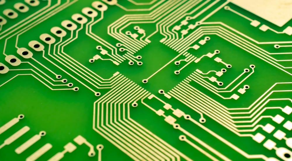
A Printed Circuit Board (PCB) is a flat board made of non-conductive material, typically fiberglass, epoxy, or composite, with conductive pathways etched or printed onto its surface. These conductive pathways, often made of copper, serve as the "wires" that connect various electronic components mounted on the board.
Construction of PCBs
Substrate Material: PCBs are typically made from a substrate material, which provides mechanical support and insulation. The most common substrate material is fiberglass-reinforced epoxy resin, known as FR4.
Conductive Layers: Thin layers of copper foil are bonded to the substrate material on one or both sides of the board. These copper layers form the conductive pathways necessary for electrical connections.
Etching or Printing: The desired circuit pattern is created on the copper layers using one of two methods: chemical etching or printing. Chemical etching involves applying a chemical resist to protect the copper that isn't part of the circuit, while printing involves directly applying conductive ink onto the substrate.
Component Mounting: Once the circuit pattern is created, electronic components such as resistors, capacitors, integrated circuits, and connectors are mounted onto the PCB. This is typically done using soldering techniques, where the leads of the components are soldered to the copper pads on the PCB.
Solder Mask and Silkscreen: A solder mask layer is applied over the copper traces to protect them from oxidation and to insulate them from accidental contact. Additionally, a silkscreen layer may be added to label component placements, reference designators, and other pertinent information.
Types of PCBs
Single-Sided PCBs: These PCBs have conductive traces on only one side of the board. They are simple and inexpensive but have limited applications due to their single-layer design.
Double-Sided PCBs: Conductive traces are present on both sides of the board, connected via plated through-holes or vias. Double-sided PCBs offer increased routing flexibility and are suitable for more complex circuit designs.
Multi-Layer PCBs: These PCBs consist of three or more layers of conductive traces separated by insulating layers. They provide enhanced functionality and are commonly used in advanced electronic devices where space is limited, and signal integrity is crucial.
Flexible PCBs: Instead of rigid substrates, flexible PCBs use flexible plastic materials such as polyimide. They are ideal for applications requiring bendability or where space constraints demand unconventional form factors.
Applications of PCBs
PCBs are integral components in a vast array of electronic devices and systems, including:
- Consumer Electronics: Smartphones, laptops, tablets, televisions, and gaming consoles.
- Automotive Electronics: Engine control units, infotainment systems, and advanced driver assistance systems (ADAS).
- Industrial Equipment: Control systems, automation machinery, and robotics.
- Aerospace and Defense: Avionics, satellites, radar systems, and missile guidance systems.
- Medical Devices: Patient monitoring equipment, diagnostic devices, and imaging systems.
Future Trends in PCB Technology
Miniaturization: With the demand for smaller and more portable electronic devices increasing, PCBs are expected to undergo further miniaturization. Advanced manufacturing techniques such as laser drilling and microvia technology enable the creation of denser circuitry on smaller PCBs.
High-Speed and High-Frequency PCBs: As data rates and operating frequencies continue to rise, PCBs capable of handling high-speed and high-frequency signals will be in high demand. Design considerations such as controlled impedance and signal integrity will become increasingly important.
Flexible and Wearable Electronics: The development of flexible and wearable electronics relies heavily on flexible PCB technology. Innovations in flexible substrates and conductive materials will drive the adoption of PCBs in wearable devices, smart textiles, and flexible displays.
Integration of Advanced Materials: Emerging materials such as graphene, carbon nanotubes, and conductive polymers hold promise for enhancing the performance and functionality of PCBs. These materials offer superior electrical conductivity, thermal properties, and mechanical strength compared to traditional materials.
In conclusion, Printed Circuit Boards (PCBs) are the cornerstone of modern electronics, enabling the creation of increasingly sophisticated electronic devices and systems. With ongoing advancements in technology and materials, PCBs will continue to evolve, paving the way for the next generation of innovative electronic applications.
Report this page